Wang 600 Zero Flag Fault
Next Log Entry
ROM Emulator Design Flaw
With suspicion firmly on the zero flag conditional execution logic, Doug Miller rapidly produced a custom microcode that tested each of the seven conditional instructions and displays the result.
The zero test did indeed fail, while the other six conditional tests passed.
Testing the Zero Test - 1
The Wang 600 ALU operates on 4-bit data items in bit-serial fashion. Testing for zero is a simple matter, setting a ‘zero’ flip-flop before a data cycle and allowing bit serial data to pass by its reset input. If the data is non-zero then the flip-flop will be reset, clearing the ‘zero’ state.

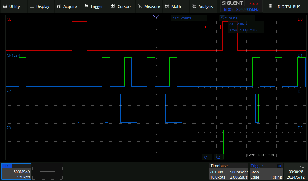
- (red) CL pulse marking the start of each microcode cycle
- (CK1234) four pulses that clock the bit-serial bus LSB->MSB
- !Z the bit-serial Z bus that carries the Z register
- Z0 the zero flip-flop, set(high) if Z is zero
The trace shows that the Z0 flip-flop is reset to non-zero state at the very start of the data cycle by a pulse that is quite short. This pulse is shorter than one of the CK1234 pulses, and its edges do not align with the major edges such as those of CK1234. This is suspicious that something ‘odd’ could be going on. Further inspection shows a very short glitch pulse on the !Z bus, mid-way through the CL pulse. This glitch is too short to originate from the clocked signals of the logic engine, and raises more concern of ‘oddness’
Testing the Zero Test - 2

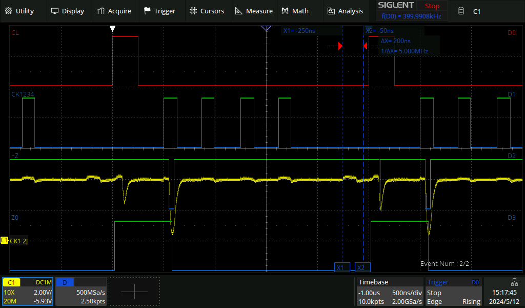


The !Z bus should remain at zero in this case but it still has the suspiciously short pulse during CK1, a pulse that has no clear relationship to the main clocking signals, but does appear to be (incorrectly) resetting the zero flip-flop.
Having found some peculiar signals on the Z bus that seemed to be unconnected to the major logic engine clocks, it was fortunate to be using the MSO rather than the 16500C Logic Analyzer. The MSO made it easy to look at the suspect pulses in analog mode, the better to assess their form and likely origin. And indeed, they were not crisp logic transitions (as the digital channels can make them appear to be). Both pulses seen on the yellow analog channel look more like glitches caused by crosstalk, interference or something similar.
Finding the Glitches
The Zbus is generated on the 5964 ALU board from a complicated tree of NANDs, NORs and XORs.
Rather than try to fathom the logic of that tree it was simpler to make use of the peculiar analog appearance of the glitches and work back through the tree, following the inputs where the characteristic glitches were present.
Kudos yet again to Douglas for noting that the glitches lined up with transitions of AOP data from the ROM emulator.
ROM Emulator Design Error
Further analysis revealed that the ROM emulator, designed several months ago in the early phase of hardware debugging, was flawed.
The emulator was using the CUP signal (which drives current in the wire ROM wires) as its primary reference for latching ROM address and enabling ROM output data. While the address latching was satisfactory under this scheme, ROM data output was not and was occurring too late. The late update of ROM data appeared to be the cause of the glitches affecting the Zbus.
Review of ROM emulator timing suggested that the CL signal was a more appropriate signal,
- latching ROM address on the leading edge of CL,
- disabling ROM output during CL and
- re-enabling ROM output on the trailing edge of CL.
The ROM Emulator was revised to use CL as its main timing reference
Previous Log Entry Back to Log Index Next Log Entry