Wang 600 Wire ROM Optimization
Next Log Entry
Understanding and optimizing the ROM and the ROM Reader
The satisfaction at restoring the KK1 column and being able to dump the complete ROM (other than the four ROM dead addresses) was tempered after discovering that successive ROM dumps had discrepancies, the ROM was not returning consistent data. After performing some dozens of complete ROM dumps and making comparisons and bit counts, some patterns could be discerned:
- most of the ROM did read consistently, but errors affected around 5% of addresses
- the same addresses appeared to be stable, or variable
- most of the errors appeared to be 1 bits reading as zero, rather than zeros reading as 1
- some bits in the ROM were much more variable than others.
These observations did not suggest any one cause for the ROM unreliability. Specific bits being more affected suggests that the sense circuits for those bits may be marginal, while certain addresses being consistently variable suggests insufficient coupling between ROM wire and sense circuit, or noise affecting the coupling.
The ROM schematic describes a number of factory adjustments to optimize ROM performance:
- ROM drive current
- ROM drive waveform
- sense circuit optimisation
ROM Drive Current
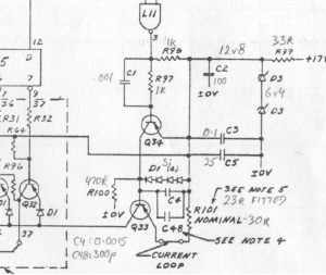

The ROM PCB had a 30R 0.5W carbon composition resistor (R101) installed. Resistors of this type are known to drift in value over decades, with higher values being worse in this regard. In the case of a 30R resistor, it does not take too many R’s of drift to change the final value quite significantly.
The current settiing resistor was removed and measured (4wire) as 26R5. This appeared to be a reasonable value and in the absence of a specific adjustment procedure, best left as it.
ROM Drive Pulse Shape
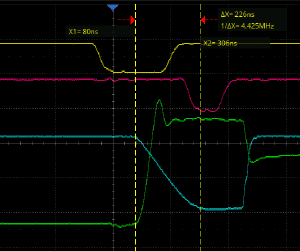

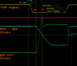

The first thought for “rise time of 200nS” was the Q33 collector signal, since this measured 150nS it appeared to be a good candidate for adjustment. Unfortunately this idea was not verified on the schematic and time was spent on fruitless adjustment of C48, then checking C4 and finally concluding that the C4-C48 combination measured 1795pF, almost exactly the nominal value of 1800pf. And adjusting these had little/no effect on Q33 risetime.
In frustration at not finding a likely cause the schematic was stared at again, until realising that C4-C48 would soften the current turn-on through Q33 and this would be reflected in the shape of the current rise time. Measuring the rise (on-screen fall) showed 226nS which was at the boundary of specification and seemed best to note and leave as is.
This left a frustrating situation with the ROM still very unstable but nothing obviously out of specification in the ROM hardware.
Wire ROM Description in Wang Patent
More information was needed about the ROM and the archives were examined again to see if any other schematics or technical data had been overlooked. The Wang 700 is the original machine with wire ROM technology and the US Patent for that machine turned out to have a reference to another Wang patent, USP3727201, that deals specifically and in detail with wire ROM technology. This patent and another concerning the machine Wang built to manufacture the ROMs, can be found in the Wang 600 Data section
The patent cites a wire drive current of 70-90 mA in a pulse of length 200-400nS with controlled rise time to reduce crosstalk. All of these criteria have been measured above and are met. The patent then describes important and subtle features:
- the output latches should be held in clear state until after the ROM drive pulse has risen
- the strobe signal must be carefully timed: after clear and coincident with the ROM drive plateau.
Review and Revision of ROM Reader

A series of revised firmwares were built, timings were adjusted according to the understanding gained from the patent, and ROM readout improved. The ROM that appeared to be finicky and unreliable was transformed into a solid and repeatable example of early memory technology.
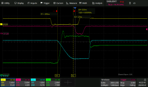
The revised reader timing is shown, note that
- CL now overlaps the rising ROM drive signal so that the output latches are not released until the ROM drive reaches steady-state and,
- ST occurs during ROM drive steady-state, after CL has ended
This appears to be a sophisticated noise cancelling technique, using two levels of gating to address two main noise sources:

- CL is used to hold the data output latches in reset state while the current pulse builds up. The rising current causes crosstalk between data wires which can cause spurious signals in the sense transformers. The rise time is controlled electronically to reduce this effect but extending the CL state until the rise time has ended provides a gate to exclude these spurious signals
- ST is used to open the data latch ‘set’ inputs only during the period when sense transformer outputs are maximal. This prevent noise pulses at other times from setting data latches.
The Data Capture traces show a read cycle, with the JL0 bit monitored on the top yellow trace. The JL0 bit begins set to 1 from the previous read cycle. It is reset to 0 by the CL signal at the start of a new read cycle, later in that cycle the ST signal opens the data latch set inputs to allow the latches to capture any ‘1’ signals being emitted by the sense transformers at that time.
This finally gave a very clean and stable read of the entire ROM.
It is now possible to dump the entire Wire ROM from machine CC2001. While there are four dead addresses, it is hoped that they can be reverse engineered, leading to full recovery of this Wire ROM.
Previous Log Entry Back to Log Index Next Log Entry