Previous Log Entry Back to Log Index

Wang 600 Wire ROM Diagnosis Next Log Entry

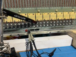
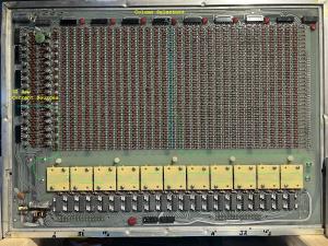
Diagnosis of Silent Column and Rows

Examination of the wire ROM image had shown that

  • Bit 1 of the KK field was zero in all ROM locations and
  • four locations read as all zeros.

The silent KK bit was an obvious fault. The silent locations were very likely faults but required critical evaluation; on the one hand the microcode is very dense and it seems unlikely that unused locations would be present but on the other hand, all-zeros is a legitimate microcode word and so could be a vaild instruction.
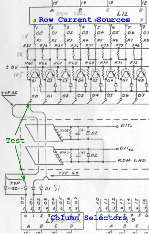
Silent KK Bit

A missing bit in all locations suggests a fault in the detection and/or latching of the output pulse from the sense coil. The circuit that performs this is simple but subtle. Essentially, an SR latch is reset at the start of each memory cycle and then the positive part of the sense coil output is rectified and used to set the latch if the corresponding bit is coded a a 1 in the ROM.


The ROM Reader was used to read from a location known to have KK bits 0 and 1 set to 1. As can be seen, the KK output latch is reset by the CL signal at the start of the memory cycle. The ST signal conditions the latch for the occurrence of a sense signal and the KK0 latch can be seen to be set by the sense pulse. For the KK1 bit however, the KK1 sense pulse does not set the KK1 output latch.


This suggested that the NOR gates forming the KK1 latch were defective. Applying the Logic Probe and Logic Pulser showed that the KK0 latch could be set and reset by pulses to the respective latch inputs. The KK1 latch could be reset but did not set in response to the Logic Pulser.

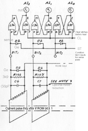
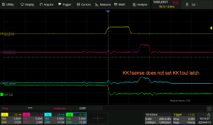
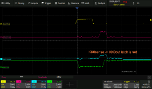
This confirmed that L26, an SP380A quad NOR was faulty.


ROM Locations Reading All-Zero

Four locations had been found to return all zeros, these were (decimal/hex):

  • 85 / 0x55
  • 584 / 0x248
  • 850 / 0x352
  • 1298 / 0x512

As noted above, it’s possible that one or more of these locations may be legitimately zero. The pathological causes of all-zeros are an open-circuit data wire or open-circuit blocking diode and these can be reasonable easily tested for, once the layout of the ROM board is understood.

The ROM board layout can be regarded as 64 X-values and 32 Y-values. The 64 X-values are decoded from the 6 lower-order ROM address bits and each X-value is connected to the cathodes of 32 diodes, seen in columns in the picture. The anode of each diode is connected to a singe ROM data wire which is threaded through the data transformer area and then terminates at one of 32 current source switches, representing the Y-values. Probing between a diode anode and transistor collector will test if a data wire is intact.

Testing the above locations showed:

  • Location 85: Wire Open
  • Location 584: Wire Open
  • Location 850: Wire Open
  • Location 1298: Wire Open

The ROM has four open wires, likely to be a very challenging repair and perhaps not possible.

Previous Log Entry Back to Log Index Next Log Entry